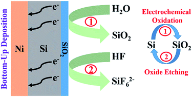
Packaging applications in the semiconductor industry rely on electrodepositing metals into high aspect ratio (HAR) vias without the formation of any defects or voids. The process and economic efficiency of conventional methodologies are limited by the ability to achieve high deposition rates along with uniformity of the deposited metal layer. In this work, a contactless and scalable electrodeposition technique has been developed to deposit metallic nickel onto p-doped silicon wafers. The effect of various process variables such as deposition and etchant solution composition and concentration, solution temperature and stirring on nickel deposition rates have been investigated. The importance of backside silicon oxidation and subsequent oxide etching on the kinetics of nickel deposition on frontside silicon has been highlighted.