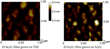
Zr-doped In2O3 (Zr-In2O3) (222) epitaxial layers of thickness 210 nm were grown on yttria-stabilized zirconia (YSZ) (111) and Al2O3 (0001) substrates with rf magnetron sputtering at 350 °C in an atmosphere deficient in oxygen. X-Ray scattering and use of a transmission electron microscope (TEM) revealed Zr-In2O3 films to be deposited epitaxially on YSZ (111) and Al2O3 (0001). Images observed with an atomic-force microscope demonstrate that the substrate profoundly affected the topography of the Zr-In2O3 (222) epilayers. The large mismatch of the Zr-In2O3 (222)/Al2O3 (0001) heteroepitaxy was responsible for the surface structure of the epilayer being rougher than that on YSZ (111). Cross-sectional TEM images reveal dense crystalline films with no macroscopic imperfection; the crystalline order of Zr-In2O3 epilayers is preserved up to the top surface. The Zr-In2O3 (222)/YSZ (111) heteroepitaxy has a Hall mobility greater than that of Zr-In2O3 (222)/Al2O3 (0001), perhaps due to the greater lattice mismatch of the Zr-In2O3 (222)/Al2O3 (0001) heteroepitaxy that results in Zr-In2O3 having a poor crystalline quality. Domain boundaries on a nanometre scale were found in the heteroepitaxial Zr-In2O3 (222)/Al2O3 (0001) resulting from random nucleation and relaxation of misfit stress. The existence of these domain boundaries on a nanometre scale thus affects the electrical properties of the Zr-In2O3 epilayer.