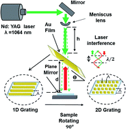
The development of accurate and rapid techniques to produce nanophotonic structures is essential in data storage, sensors, and spectroscopy. Existing bottom-up and top-down approaches to fabricate nanophotonic devices are high cost and time consuming, limiting their mass manufacturing and practical applications. Here, we demonstrate a strategy to rapidly create 25–40 nm thick 1/2D Au–Ti nanopatterns using holographic direct laser interference patterning (DLIP). Pulses of an Nd:YAG laser (1064 nm) in holographic Denisyuk reflection mode were used to create ablative interference fringes. The constructive interference antinode regions of the standing wave selectively ablated a Au–Ti layer in localized regions to controllably form nanogratings. Varying the laser exposure parameters allowed for rapid patterning of 2D square and rectangular arrays within seconds. Controlling the distances between the laser source, recording medium, and the object, allowed for achieving a 2D spatial grating periodicity of 640 nm × 640 nm. Diffracted and transmitted light spectra of 2D nanostructure arrays were analyzed using angle-resolved measurements and spectroscopy.