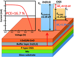
To minimize carrier recombination at interfaces and maximize the open circuit voltage and resultant power conversion efficiency, it is imperative to characterize and optimize the heterointerfaces of Cu(In,Ga)Se2 (CIGS) thin film solar cells. In this study, we investigated the surface chemical and electronic structure of CIGS with In-final and Ga-final co-evaporation processes and observed that the In-final CIGS contained larger grains and showed a slightly larger bandgap than the Ga-final CIGS. We also analyzed the band alignment of the heterointerface consisting of the Zn(O,S) buffer layer/CIGS deposited by atomic layer deposition using X-ray photoelectron spectroscopy. We found that a S stoichiometric concentration of less than 20% in Zn(O,S) is essential to achieve a power conversion efficiency (PCE) of ∼16.7% with conduction band offsets at 0.53 eV with 14% of S content. However, when the S content exceeded 20%, no PCE was obtained with conduction band offsets at >1 eV. Therefore, this study suggests that an appropriate S content in the Zn(O,S) buffer layer is a key factor for achieving improved PCE in Zn(O,S)/CGIS thin film solar cells because the carrier injection at this interface is very strongly affected by the interfacial conduction band offset.