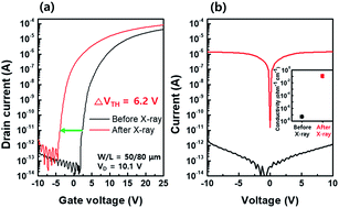
We investigated the effects of X-ray irradiation on the electrical characteristics of an amorphous In–Ga–Zn–O (a-IGZO) thin film transistor (TFT). The a-IGZO TFT showed a negative threshold voltage (VTH) shift of −6.2 V after 100 Gy X-ray irradiation. Based on spectroscopic ellipsometry (SE) and X-ray photoelectron spectroscopy (XPS) analysis, we found that the Fermi energy (EF) changes from 2.73 eV to 3.01 eV and that the sub-gap state of D1 and D2 changes near the conduction band minimum (CBM) of the a-IGZO film after X-ray irradiation. These results imply that the negative VTH shift after X-ray irradiation is related to the increase in electron concentration of the a-IGZO TFT active layer. We confirmed that the sources for electron generation during X-ray irradiation are hydrogen incorporation from the adjacent layer or from ambient air to the active layer in the TFT, and the oxygen vacancy dependent persistent photocurrent (PPC) effect. Since both causes are reversible processes involving an activation energy, we demonstrate the VTH shift recovery by thermal annealing.