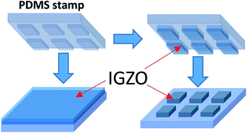
An indium gallium zinc oxide (IGZO) layer was patterned and thin-film transistors (TFTs) were fabricated by surface modified polydimethylsiloxane (PDMS) stamping and IGZO solution. The PDMS stamp was prepared by immersion in piranha solution and treatment with UV–ozone to make a hydrophilic surface. Patterned PDMS was inked by contact with the IGZO layer, and then stamped on the desired substrate. The process did not cause etching damage, so the stamped amorphous-IGZO TFTs showed low leakage current of ∼10−11 A, high on/off current ratio of ∼108, carrier mobility of 6 cm2 V−1 s−1, and narrow hysteresis of 0.2 V. UV irradiation on the IGZO layer caused a photochemical annealing effect that improved the electrical properties of IGZO TFTs. This method provides a simple and versatile process to fabricate transparent metal-oxide TFTs based on patterning the devices by reusable stamping methods.