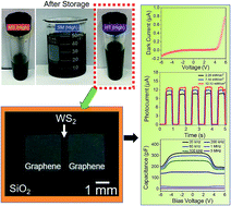
In the present work, various chemical exfoliation routes for semiconducting two-dimensional (2D) layered material WS2 are explored, which include magnetic stirring (MS), shear mixing (SM), and horn-tip (HT) sonication. Current–voltage measurements, Raman spectroscopy, and photoluminescence (PL) spectroscopy were used to characterize the drop-casted WS2 nanosheets produced by these three techniques and our analysis revealed that HT sonication produced the most optimal dispersions. Heterostructure photodetector devices were then fabricated using inkjet printing of the HT sonicated dispersions of WS2 and graphene. The photodetector device performance was measured using a stream of ON/OFF light pulses generated using a red laser with wavelength λ ∼ 660 nm, and an arbitrary waveform generator. From this analysis, the photoresponsivity and detectivity of the graphene–WS2–graphene heterostructure devices were calculated to be ∼0.86 A W−1 and ∼1013 Jones, respectively. Capacitance–voltage (C–V) and C–frequency (f) measurements were also conducted, where the V was swept from –6 V to +6 V, while the change in C was measured from f ∼ 20 kHz up to 3 MHz to gain insights into the nature of the graphene–WS2 interface. From the C–V measurements, the C plateaued at ∼324.3 pF from ∼−4 V to +4 V for the lowest f of 20 kHz and it reduced to ∼200 pF from −6 V to ∼−4 V, and similarly from ∼4 V to 6 V, C was ∼190 pF. The decrease in C for V > +4 V and V < −4 V was attributed to the reduction of the interfacial barrier at the electrodes which is suggestive of a Schottky-based photodiode at the graphene–WS2 interface. A sharp decrease in C from ∼315.75 pF at 25.76 kHz to ∼23.79 pF at 480 kHz (at 0 V bias) from the C–f measurements suggests a strong effect of interface trap density on C built-up at the graphene–WS2 interface and the ensuing Schottky barrier height. Our work confirms the excellent potential of solution-cast, trilayer graphene–WS2–graphene heterostructures as a promising photodetector platform using additively manufactured inkjet printing.